Clocks, Signals, and Delays
Digital circuits are invariably controlled by a clock and events take place at discrete points in time. This article looks at several topics related to the clock and the propagation of signals through a digital system. In principle, you shouldn’t have to worry about clock signals and delays. All you should have to do is to create a digital circuit that performs the appropriate digital function. In practice, signals are delayed as they pass through circuits and two signals may even arrive at a given point out of sync with each other, if they have taken different routes. Designing a circuit today is as much about satisfying timing constraints as it is about satisfying Boolean constraints.
Fortunately, most computer users don’t have to worry about clocks and timing. Such worries are the province of the electronic engineer and circuit designer. However, as a student of computer architecture it is necessary to appreciate the need for accurate timing.
We are going to look at the following topics:
- the clock that generates a sequence of equally-
spaced pulses - the structure of the waveform generated by a clock
- the behaviour of pulses in circuits
- hazards, glitches, and race conditions
- setup and hold times
- metastability
The Clock
The clock is a circuit that provides a sequence of pulses to trigger each internal operation. The digital clock in a computer is the same as the digital clock in your watch, albeit operating at a much higher rate.
A clock may operate at the basic instruction rate of a computer, or a multiple of the instruction rate because each instruction may itself be executed as a series of partial instructions or microinstructions.
Figure 1 illustrates the waveform from a perfect hypothetical clock. We assume that the pulses are perfectly uniform and equally spaced. Moreover, they have zero rise and fall times; that is, the transition from a 0 state to a 1 state and from a 1 state to a zero state is instantaneous. Finally, when the clock is in a zero state, the signal is constant and when the clock is in a 1 state it is similarly constant; that is, the waveform is perfectly square.

Figure 1 The Perfect idealized clock
If we assume that the up time and down time (high to low time) is constant and 1:1, the only parameter that describes a clock is its frequency; that is, the number of transitions per second. In the early days of the microprocessor, typical clocks ran at 1 MHz (1,000,000 transitions per second). Today, clock frequencies of 1 GHz, 1,000 million of 109 transitions/second are common.
Another parameter of a clock (in figure 1 tcyc) is its cycle time, of the duration of a clock cycle. This is the reciprocal of the frequency; that is, tcyc = 1/F. A 1 MHz clock has a cycle time of 1/106 = 1/1,000,000 = 1 ms. A 1 GHz clock has a cycle time of 1/109 = 1 ns. One nanosecond is such a short interval that light travels only one foot (30 cm) in 1 ns.
Often a clock has a perfectly symmetric waveform with equal up (logic 1) and down times (logic 0). However, not all clocks (or pulse sequences) have identical up and down times. Figure 2 illustrates such a waveform.

Figure 2 Pulse sequence with different up and down times
The ratio between the up and down times is called the mark:space ratio (the term
comes from the pre-
In practice, waveforms are never perfect. Figure 3 illustrates a waveform with sloping rising and falling edges. Signals never make instantaneous 0 to 1 and 1 to 0 transitions and an edge can be characterized by its rise time and fall time. Note that the rise/fall ime is usually measured between tow specific points; for example, 10% and 90% of the peak level.

Figure 3 Clock signal with rising and falling edges
We can introduce a further level of imperfection called jitter. The term jitter refers
to random variations in the time at which an edge makes its transition. In a perfect
world this would be 0. In everyday terms, if you aim to arrive at the office at 8.50
every morning but you arrive anywhere between 8.45 and 8.57, the random variation
of -
Figure 4 illustrates the concept of jitter. He trace shows a clock making a negative transition after its nominal transition point. Jitter is typically random and its distribution (jitter value plotter against probability) follows a Gaussian curve. The curve in figure 4 also illustrates the concept of the Gaussian variation in jitter.
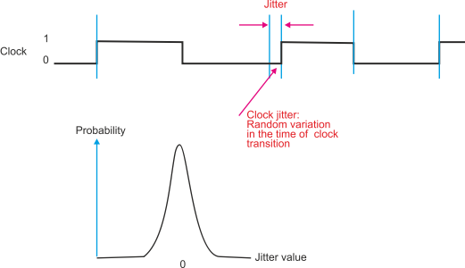
Figure 4 Clock signals with jitter
Figure 5 illustrates a real-
Overshoot: the signal goes above the 1 level on a positive transition
Undershoot: the signal goes below the 0 level on a negative transition
Ringing: the signal oscillates at the beginning or end of a transition
Droop: the signal does not maintain a steady level between transitions.
Noise: Noise if the effect of extraneous random signals superimposed on the clock signals
All these effects are bad and can contribute to incorrect operation and random errors. In a marginal design, such errors may occur very infrequently and be difficult to debug.
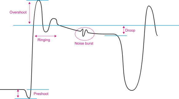
Figure 5 Real world clock signal
Propagation Delay
When a signal is applied to the input of a circuit, the output does not change until after a finite time, the propagation delay. Figure 6 illustrates the propagation delay through a simple invertor. Although we speak of propagation delay, the delay experienced by a 0 to 1 transition may not be the same as that experienced by a 1 to 0 transition.
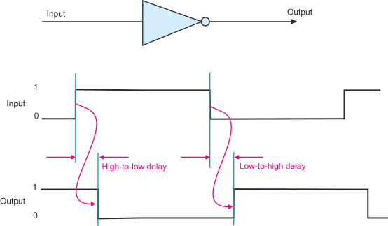
Figure 6 Propagation delay through an invertor
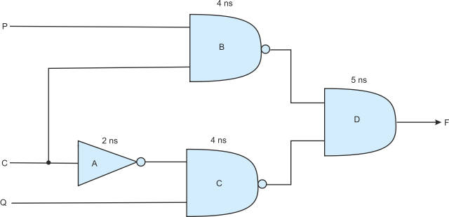
Figure 7 illustrates a logic circuit with four gates. This is a 2-
When computing the worst-
Figure 7 Delay in a logic circuit
The Glitch
The term glitch indicates a short-
Figure 8 illustrates the concept of a glitch with a simple two-
However, if you look at the timing diagram, you with see that there is a short term positive pulse, the glitch caused by the propagation delay through the invertor.
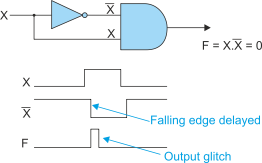
Figure 8 The Glitch
Delays in circuits caused by propagation paths through logic elements or even the propagation delay incurred by interconnections can lead to incorrect or intermittent operation. Logic design techniques, the control of signal path lengths and synchronization circuits can all bee used to minimize the problems of signal delay.
Setup and Hold Times
Two very important timing parameters of clocked circuits with latches are setup and
hold times. Consider the D flip-
The same criterion must be applied to the flip-
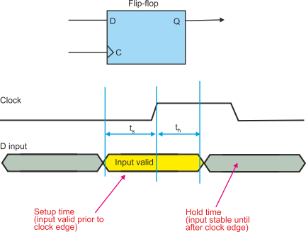
Figure 9 Set up and hold time
As well as setup time, an input must also comply with a hold time. Again, consider the everyday case. In the good old days (i.e., prior to PowerPoint) I could draw a figure on the blackboard and the students were able to write it down (well, at least the students where were (a) awake and (b) actually cared about what I was doing). With the advent of PowerPoint, I get a chorus of “Wait, I haven’t finished yet” every time I move on to the next slide. Providing information is not enough, you have to provide sufficient time for that information to be captured. This is, of course, the hold time. When an input is clocked, the input must be stable of a minimum hold time before which it can begin to change, figure 9.
Consequently, the minimum time for which any signal must be valid is the sum of its setup and hold times.
Tri-
A tri-
The purpose of a tristate gate is to allow multiple logic devices to drive the same
bus. Processors, memory devices, bus drivers etc, frequently have tri-
The most significant aspect of tristate design is that you must never, ever have two tristate outputs attempting to drive the same bus at the same time. For example in a memory array, only one chip at a time can drive the common bus.
Figure 10 illustrate the timing of a tristate driver. We assume that this driver
is enabled by an active-
When the enable signal returns inactive-
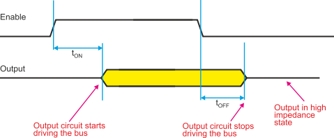
Figure 10 Tri-
If is easy to control tristate drivers; for example, a 3-
However, life is not that simple. It takes time to turn off a tristate driver and it takes time to turn on a tristate driver. Consider figure 11 where two tristate drivers are connected to the same bus.
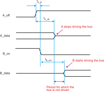
Figure 11 Driving a bus
In this example, device A is initially driving the bus. When its control signal goes inactive high (notice that the active state in this example is low which is traditional) A stops driving the buss after tA_off. Device B then begins to drive the bus tB_ON after the assertion of its control signal.
In figure 11 there is a gap between the point at which the bus is turned off by A and the point at which the bus is turned on by B. For proper circuit operation this gap must always be positive. However,, if it is negative and A turns off after B turns on, glitches are possible and the tristate outputs could even be damaged physically by allowing high currents to flow through two gates in series.
Clearly, it is necessary that tA_B + tB_ON > tA_OFF